Affiliate links on Android Authority may earn us a commission. Learn more.
Pixel Visual Core: A closer look at Google's hidden chip

Back with the launch of Google’s Pixel 2 and Pixel 2 XL, it was revealed that Google included an extra chip in the phone alongside the main processor. Known as the Pixel Visual Core, the chip is aimed squarely at enhancing the phone’s image processing capabilities. The chip has returned once more inside Google’s latest Pixel 3 and 3 XL.
According to Google, the secondary chip is designed to compile HDR+ images 5 times faster than an application processor — with 1/10th the power consumption. The Pixel Visual Core also handles complex imaging and machine learning tasks related to the camera, which includes auto image adjustments based on the scene, among other uses.

Pixel Visual Core was enabled in the Pixel 2 with the arrival of the Android 8.1 developer preview. The Pixel Visual Core is the company’s first piece of custom-designed silicon to make its way into a smartphone, giving the company tighter control over its phone’s capabilities than ever before.
Two SoCs in one phone
Machine learning and a heterogeneous approach to computing — using dedicated hardware to perform certain tasks more efficiently — aren’t new concepts in the smartphone space. SoC manufacturers like Qualcomm have been pushing processing in this direction for a couple of generations and already include dedicated image signal processor (ISP) and digital signal processor (DSP) components inside its flagship Snapdragon series. You’ll find all of this inside the new Pixel phones. Qualcomm is already targeting these components for power efficient use with machine learning, image processing, and data crunching tasks. Clearly, Google wants to augment or surpass these capabilities.
Opting for a stand-alone processing unit is an unusual choice, suggesting that Google wants to seriously augment the main processor's built-in DSP capabilities.
Google opting for an additional, stand-alone Image Processing Unit (IPU) is an unusual choice. Ideally, these components should be closely integrated with the CPU and GPU to avoid any latency issues transferring data in and out of the processor. However Google can’t build any custom silicon into Qualcomm’s design, the only option for custom hardware is to design a secondary stand-alone SoC to communicate with the main application processor, and that’s exactly what the Vision Core does.
A look inside the Pixel Visual Core
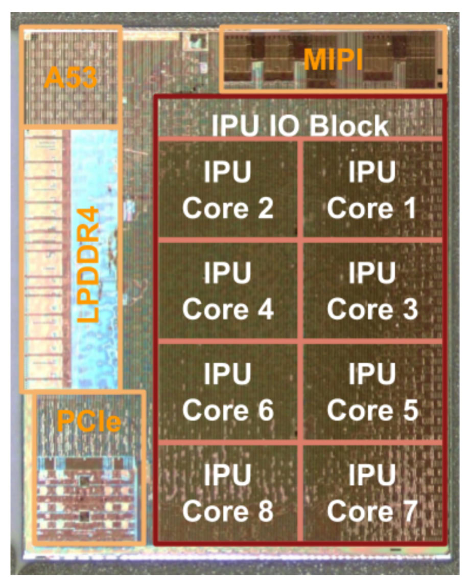
Before even looking at the processing capabilities of the new core, there are a few telltale signs of its standalone design. There’s onboard LPDDR4 RAM to quickly read and write data without having to go to main memory, along with a PCIe bus connection for talking to an external processor. A single Cortex-A53 CPU hands incoming and outgoing communications to the main application processor.

On the image processing side, the chip consists of eight IPU cores. Google states that each of these cores packs in 512 arithmetic logic units (ALUs), granting the ability to perform more than 3 trillion operations per second in a mobile power budget. Each core is designed for multiply-accumulate, a common machine learning function. For comparison, a Cortex-A73 CPU core inside a high-end mobile application processor only contains two basic integer units, along with load/store and FPUs.
Even with heavily optimized SIMD extensions, you would be lucky to maximize all of those capabilities at once on a CPU. A dedicated mass math processor will simply be faster at specific operations. The Visual Core appears is specifically designed to perform mass math operations across the millions of pixels in a picture, so this type of setup can be well utilized for imaging tasks. In a nutshell, the Pixel Visual Core takes in lots of pixel data from the camera and computes new pixels for the best looking output. A CPU has to deal with a wider range of possible operations, so a 512 ALU design wouldn’t be practical or useful for general applications.
With 512 ALUs in each IPU core, Google's Visual Core is designed for mass parallel math, perfect for image processing and mass neural networks.
Google also states that a key ingredient to the IPU’s efficiency is the tight coupling of hardware and software. Google’s software for the Pixel Visual Core can apparently control many more details of the hardware than in a typical processor, making it quite flexible and efficient. This comes with expensive programming complexity. To assist developers, a custom Google-made compiler is used for optimization, and developers can make use of Halide for image processing and TensorFlow for machine learning.
In summary, Google’s Visual Core can crunch a lot more numbers and perform many more mathematical operations in parallel than your typical CPU. Camera imaging data arriving as 10, 12, or 14-bit tone data spread across the Pixel 2’s 12.2 megapixel camera resolution requires wide, parallel processing for color, noise reduction, sharpening, and other data processing. Not to mention newer and more advanced HDR+ and other algorithms. This very wide ALU-heavy design is also well suited to machine learning and neural networking tasks, which also require the crunching of lots of small numbers.
Google’s image processing capabilities
Google has been using intensive image processing algorithms for a number of generations now, even before the Pixel Core. These algorithms run faster and more efficiently using Google’s custom hardware.
In a blog post, Google outlined its use of aligning and averaging multiple image frames to construct high dynamic range pictures from a short burst of images. This technique is used on all recent Nexus and Pixel phones that offer an HDR+ shooting mode. After revealing more details, the company states that its 28nm Pixel Visual Core is 7 to 16 times more energy efficient at align, merge, and finish tasks than a 10nm mobile SoC.
Google is also using machine learning and neural network algorithms for other camera software effects too. When creating a depth of field effect from a single image sensor, a convolution neural network, trained on almost a million pictures of faces and bodies, produces a mask of foreground and background content. This is combined with depth map data calculated from the Phase-Detect Auto-Focus (PDAF) dual-pixels located in the image sensor and stereo algorithms to further detect areas of the background and how much blur to apply based on distance from the foreground. This is actually the computationally intensive part. Once this has all been brought together and calculated, a disk-shaped bokeh blur is applied at each depth level to finalize the image.
Wrap up
Google’s impressive photography results in its Pixel smartphones are a major selling point for the company. It’s apparent that the company has made significant investments not only in software algorithms for improving image quality but also into hardware solutions. Not only will the Pixel Visual Core tucked inside to the new Pixels improve the performance and power efficiency of Google’s existing photography algorithms, but it could also enable entirely new features, in time.
With access to huge amounts of cloud data and content for neural network training, Google has been able to offer image enhancement software unmatched by other smartphone OEMs. The introduction of its own hardware suggests that Google may already be pressing up against the limits of the hardware that other companies can offer. A custom hardware solution better allows the company to tailor its products to its software capabilities. Whether or not Google will decide to expand its hardware development into other areas of smartphone processing in the future remains an interesting and potentially industry-shaking prospect.
Thank you for being part of our community. Read our Comment Policy before posting.