Affiliate links on Android Authority may earn us a commission. Learn more.
Beyond 7nm - the race to 4nm is Samsung's to lose

7nm manufacturing lines from TSMC, Samsung, and GlobalFoundries are all expected to be up and running next year, ready to roll out more efficient processors and other ICs for next generation products. Intel is running slightly behind, but is also investing heavily in the node. This shrink down to smaller and smaller transistors has also led to a contraction in the number of players participating in the race to more compact chips, as the costs of research, development, and manufacturing equipment continues to increase. Nevertheless, that hasn’t deterred some silicon manufacturers from investing huge sums in research to reach even smaller transistor sizes. 7nm may not be arriving until next year, but the race for 4nm is already underway.
TSMC, which is leading the way with 7nm, is targeting trial production of its 5nm process sometime in 2019, although it could be 2020 or later before we see any commercial chips. GlobalFoundries is right behind TSMC on 7nm, but appears to be staying put at this node for a while, with three generations planned as the company rolls out its EUV technology. Its 5nm plans might not arrive until 2021. Meanwhile, Samsung has a much more aggressive strategy thanks to its early investments in EUV technology for 7nm, and could race ahead of the competition if it sticks to schedule.

At this year’s ARM TechCon, Samsung Electronics re-clarified its ambitions for 7nm technology in 2018, followed up quickly by a move to 6nm, 5nm, and even 4nm by as early as 2020. This is a more ambitious deadline than most of its competitors, with TSMC coming the closest. Although it is possible that Samsung’s plans, just like its rivals’ ambitions, could end up being pushed back.
Extreme Ultraviolet Lithography (EUV)
As we approach next year’s 7nm chips, we’re hearing more about Extreme Ultraviolet Lithography research, development, and manufacturing equipment. Samsung is moving straight to EUV technology when it jumps to 7nm next year, while GlobalFoundries and TSMC won’t be. These two will be sticking with immersion lithography for their first generation 7nm processes, before moving on to EUV for second generation designs.
As foundries look to push below 5nm, EUV is an essential investment. The smaller component sizes are already stretching the accuracy, production speeds, and cost efficiency of traditional lithography techniques. Switching to EUV and its use of small wavelengths for superior etching at small sizes helps to solve the accuracy issue at smaller nodes, and also, in the long term, can offer efficiency and cost improvements. Samsung’s early adoption of EUV has given it a head-start in this regard, so its manufacturing techniques should mature faster in the race to enable 6nm and below.
Samsung is adopting EUV quicker than its competitors, giving its foundries a head-start as they transition past 7nm.
To reach 5nm and 4nm nodes, silicon wafer manufacturers are not only embracing EUV technology but are also looking to move beyond today’s fin field effect transistor (FinFET) designs to sidestep the issues associated with ever-smaller transistors.
Moving beyond FinFET
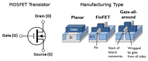
For those unfamiliar with silicon transistor technology, the processor inside your phone is built using field effect transistors (MOSFETs). Transistors work by passing current between the source and drain, which is controlled by the voltage and current applied at the gate. Toggling the gate turns the transistor on or off. In a processor, these transistors can be constructed in different ways to ensure correct current flow through the channel and keep power consumption low.
What we’re measuring in terms of nano-meters (nm) is the smallest feature size of a chip that can be manufactured using any given technique. This is usually the MOSFET gate. Typically, the smaller the transistor, the more you can fit into a chip, lowering silicon costs and providing potential energy efficiency savings thanks to lower gate voltages due to close proximity of the transistors. However, shrinking this size presents challenges to maintaining sufficient electrostatic control to toggle the channel, and offering consistent performance across the chip as the transistors becomes smaller.

As today’s FinFET designs become increasingly thin, variations in the channel width can cause undesirable variability and weaker electrostatics, potentially preventing the transistors from working as desired. To avoid these issues, engineers are looking to new transistor designs, with many viewing Gate-All-Around (GAA) FET as the best solution at sub 7nm.
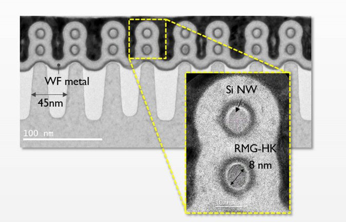
GAAFET addresses these issues by increasing the transistor’s gate surface area with the channel, providing the greatest capacitive coupling between the gate and the channel. FinFET was the first step in this direction by offering two points of gate contact, on the left and right sides of the fin. In GAAFET, a channel nanowire is sandwiched through the gate, like if a FinFET was turned on its side. Not only does this provide an all around contact area, but the technology also effectively introduces multiple gates, usually two to four, with which to control the current flow through the transistor. The theory is that this will provide more consistent variability performance.

Samsung and GlobalFoundries, in partnership with IBM, unveiled the world’s first 5nm silicon chip based on EUV technology and GAAFETs earlier in the year. In Samsung’s recent roadmap, the company is expecting to debut GAA technology by the time it reaches 4nm, replacing FinFET which will likely be exhausted after 5nm, even with new materials. The downside of GAAFETs is that the nanowiring is more difficult to manufacture than traditional FinFETs, and the process will therefore be much more expensive.
Wrap Up
Even though consumers won’t benefit from 7nm chips until 2018 or 2019, deployment of the essential technologies to shrink chips down even further is already well underway. Samsung has been very vocal about its plans and seems confident in its EUV and GAAFET road map to reach 4nm ahead of the competition. It may need the win, as TSMC is expected to win the race to 7nm.

All that said, Samsung isn’t the only foundry working with EUV and GAA technologies, and we will almost certainly see efforts from these other companies come to light in the next year or so. Samsung has come out with its ambitious plans very quickly, but delays and hiccups aren’t uncommon in the foundry business. We’re still waiting to hear more details about sub-7nm from TSMC and GlobalFoundries, who may not be too far behind. Of course, there’s a lot more to building the best chips than simply reaching a smaller node first.
Regardless, Samsung certainly looks to be pushing ahead quickest. Based on its projections, the company could break away from the competition as early as 2020. The race to 4nm appears to be Samsung’s to lose.