Affiliate links on Android Authority may earn us a commission. Learn more.
Snapdragon 835 unveiled - Everything you need to know
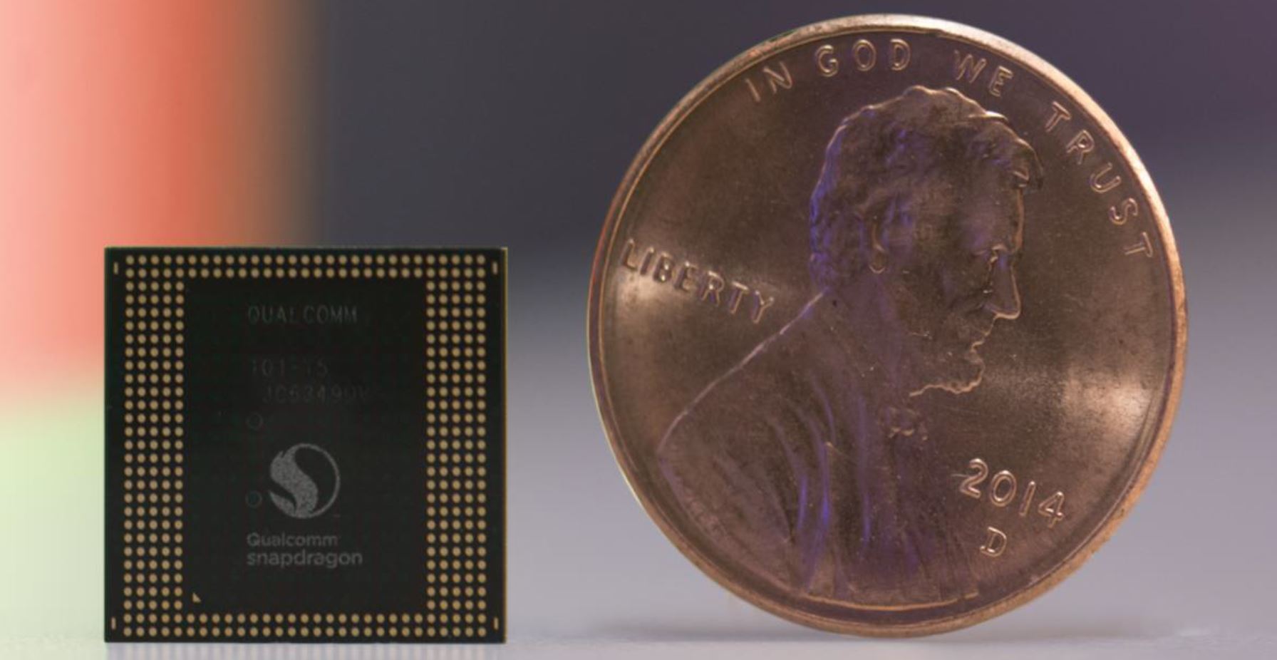
Back in November, Qualcomm unveiled the name of its 2017 flagship mobile applications processor, the Snapdragon 835, and today the company has announced the key details and features of its latest mobile SoC. In addition to the anticipated performance improvements, Qualcomm is opening up new avenues to OEMs with advanced imaging, display, and machine learning capabilities, among others, which are all exciting prospects for future mobile devices.
Sticking with the processing hardware for now, there have been some notable changes to the Snapdragon 835’s CPU configuration compared with last year. An octa-core configuration returns, after the Snapdragon 820 swapped back to a quad-core design, but the biggest change is with the new Kryo 280 CPU architecture. Despite the similar names, the Kryo 280 is a semi-custom CPU design based on an unspecified ARM Cortex core, possibly the Cortex-A73 although Qualcomm has not revealed the specifics. The original Kryo cores inside the Snapdragon 820 were a complete Qualcomm custom solution, while the older 810 opted for stock ARM parts. The new Kryo 280 CPU core is used in both the “Performance” and “Efficiency” core parts of the CPU, with 2.45 and 1.9 GHz clock speeds respectively.
| Snapdragon 835 | Snapdragon 821 | Snapdragon 810 | |
|---|---|---|---|
CPU Core | Snapdragon 835 Semi-custom ARM Cortex | Snapdragon 821 Kryo | Snapdragon 810 ARM Cortex (ARMv8) |
CPU Config | Snapdragon 835 4x 2.45GHz Kryo 280 4x 1.9GHz Kryo 280 | Snapdragon 821 2x 2.35GHz Kryo 2x 1.6GHz Kryo | Snapdragon 810 4x Cortex-A57 4x Cortex-A53 |
GPU | Snapdragon 835 Adreno 540 | Snapdragon 821 Adreno 530 | Snapdragon 810 Adreno 430 |
DSP | Snapdragon 835 Hexagon 682 with HVX | Snapdragon 821 Hexagon 680 | Snapdragon 810 Hexagon V56 |
RAM | Snapdragon 835 2x 32-bit LPDDR4X 1866 MHz | Snapdragon 821 2x 32-bit LPDDR4X 1866 MHz | Snapdragon 810 2x 32-bit LPDDR4 1600 MHz |
Flash | Snapdragon 835 eMMC 5.1/ UFS 2.1 | Snapdragon 821 eMMC 5.1/ UFS 2.0 | Snapdragon 810 eMMC 5.0 / UFS 1.0 |
Process | Snapdragon 835 10nm FinFET | Snapdragon 821 14nm FinFET LLP | Snapdragon 810 20nm HPm |
Qualcomm is keeping the exact details of its custom CPU design a secret, but has suggested that the licensing arrangement from ARM allows the company to make key changes to the execution pipeline and branch prediction, among other inner workings. ARM announced its custom CPU core licensing option back in May of 2016 and Qualcomm is the first processor company to bring a product to market using a semi-custom ARM Cortex CPU.
Qualcomm aims to have up to 80 percent of a smartphone's processing done on just the 835's low power CPU cores.
In terms of performance, Qualcomm suggests a notable 20 percent boost over the 820, and the increased number of cores suggests that most of the gains will come in the form of multi-processing capabilities. As we’ve seen from other SoC and CPU designers, the main aim with the Snapdragon 835 is to greatly improve energy efficiency, allowing for sustained peak performance and longer lasting battery life.
The company expects that smartphone power users will see an extra 2.5 hours’ worth of battery life when compared with the Snapdragon 820, and energy consumption is now just half that of the old Snapdragon 801. This is partially aided by Qualcomm’s choice of Samsung’s second generation 10nm FinFET manufacturing node. According to Samsung, the move to 10nm provides approximately a 30 percent increase to area efficiency, combined with up to a 27 percent boost to performance or a 40 percent reduction in power consumption compared to 16nm.

Before we move on from CPU details, Qualcomm has upped the amount of L2 cache quite a bit this time around, with 2MB available for the high performance cores. Surprising, the smaller lower clocked core arrangement comes with its own 1MB of L2 cache, which will reduce the amount of calls being made to the main memory for increased performance and lower power consumption on these cores too. Qualcomm aims to have up to 80 percent of a smartphone’s processing done on just these low power cores, so we can understand why the company has beefed up this configuration quite substantially.
Even more cores for better efficiency
While the new semi-custom Kryo 280 CPU cores are an instantly notable change from last year, Qualcomm has been busy making big improvements to a number of other components inside its SoC too.
On the GPU side, Qualcomm’s latest SoC features an upgraded Adreno 540 graphics processor. This is based on the same architecture as the Adreno 530 from last year, but features a number of improvements, such as faster trilinear filtering and GPGPU compute, and boasts a 25 percent gain to 3D rendering performance over the 530, which is a notable boost. The Adreno 540 also fully supports the DirectX 12, OpenGL ES 3.2, OpenCL 2.0, & Vulkan graphics APIs, as well as Google Daydream VR platform.
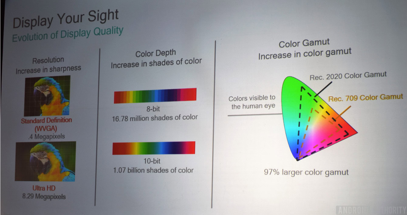
The Adreno 540’s display (DPU) and video (VPU) processing capabilities have also been upgraded to support 10-bit color. The number of supported colors jumps from 16.8 million to 107.4 million, a 64 fold increase. This opens the door for OEMs to implement HDR10 capable displays to make the most of HDR video and images. The DPU supports 10-bit color at resolutions up to 4K at 60fps.
The display processing unit also introduces an important new feature called Q-Sync. Must like NVIDIA’s G-SYNC technology and AMD’s support of the FreeSync standard, Qualcomm’s Q-Sync allows for a display’s refresh rate to be linked to the frame rate output from the GPU, if the display also supports the technology. This can greatly smooth out the appearance of the frame-rate and make jitters less noticeable when games drop frames. This is a particularly promising inclusion for virtual reality applications, as it can help to avoid motion sickness when frame rates temporarily drop.
The chip’s Hexagon DSP co-processor has also received an upgrade. As well as a more power Hexagon 682 core and the low power All-Ways Aware processor, Qualcomm has included a new HVX DSP, which is capable of handling heavy imaging and video processing tasks quickly and efficiently. This all ties in to Qualcomm’s even bigger focus on heterogeneous compute capabilities this time around, which the company first introduced with its Snapdragon 820 SoC. Tying these various cores together, along with the image sensor, display, audio, and security modules which we’ll cover later, is Qualcomm’s upgraded Symphony System Manager. This is designed to simplify heterogeneous programming in optimize performance and power consumption across the Snapdragon 835’s various processing capabilities.
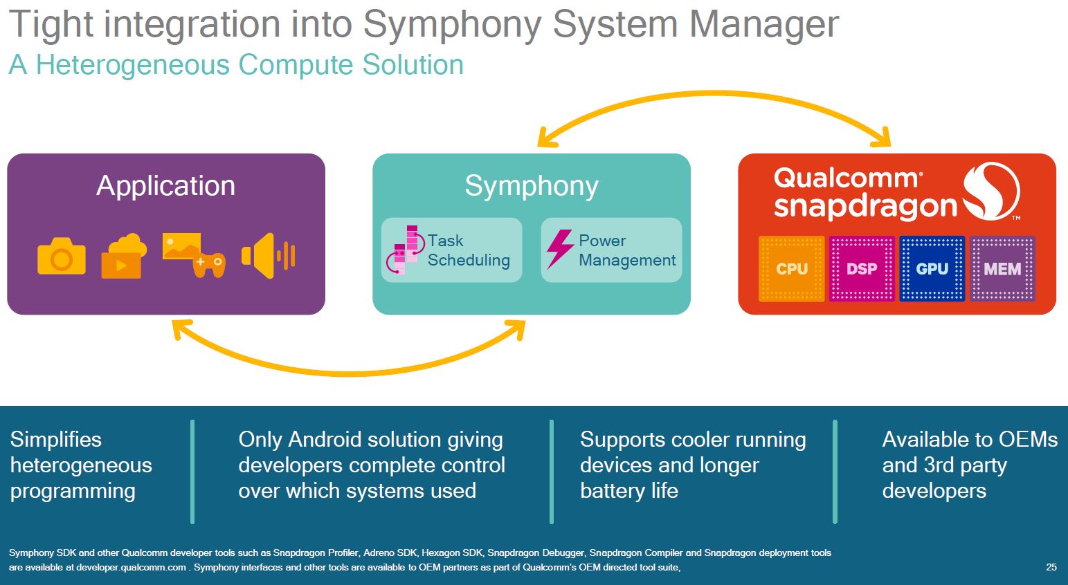
The Symphony System Manager goes beyond the CPU core schedulers that we’ve seen used in the past to balance workloads across the CPU. Symphony is actually accessible to OEMs and third party app developers, allowing them to optimize software specifically performance for Qualcomm’s latest chip. For example, specific tasks can be locked to certain CPU cores, and developers will have control over scheduling DSP and memory tasks, which could offer significant performance and battery life gains for intensive applications, such as virtual reality, imaging, and video processing. Developers don’t have to use Symphony though, Qualcomm is simply making the option available to those who need to eke out additional performance from the Snapdragon 835.
In addition to the new and improved CPU, DSP, and GPU cores, Qualcomm continues to support fast LPDDR4X random access memory in a dual 32-bit configuration with the same 1866 MHz clock speed as last year. Flash memory support has been updated to include UFS 2.1 as well as eMMC 5.1. UFS 2.1 isn’t any faster than UFS 2.0, both peak at 1.2GBps transfer speeds, but the revision lowers power consumption and provides additional data security through the use of inline cryptography between the SoC and UFS Storage device.
Enriched multimedia
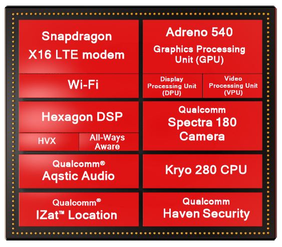
Qualcomm has also made a major upgrade to the Snapdragon 835’s image processing capabilities. The SoC’s Spectra ISP still support Qualcomm’s Clear Sight technology for color and monochrome sensor combinations for better contrast and noise, but the ISP now also supports the Snapdragon Optical Zoom module, which as the name suggests brings 2x optical zoom capabilities and an improved 10x digital zoom to the platform. This technology works using a telephoto lens alongside a wide-angle lens. Of course, it will be up to handset manufacturers to implement these features, but support in the SoC will make development more cost effective and simplified. Spectra remains a 14-bit dual ISP setup that supports up to dual 16MP cameras or a single 32MP sensor.
Support for the Snapdragon Optical Zoom module brings 2x optical zoom capabilities and an improved 10x digital zoom to the Snapdragon 835, in addition to dual RGB/monochrome setups via Clear Sight.
That’s not all, Qualcomm has also integrated Electronics Image Stabilization (EIS) 3.0 and Dual Photodiode Auto-Focus (2PD) support into the module. EIS 3.0 provides more efficient gyro sensor sampling and smoothing algorithms, supports resolution up to 4K, and combines with heterogeneous compute capabilities for more power efficient video stabilization. 2PD allows for image sensors to feature phase detection diodes in every pixel, rather than just 5% of them, which greatly improves the speed and accuracy of PDAF. We originally saw this technique inside the Galaxy S7 using Samsung’s own technology.

Moving away from the processing side, the Snapdragon 835 comes with support for Qualcomm’s revised Quick Charge 4.0 standard. Quick Charge 4.0 remains backwards compatible with the previous releases, but now also plays nice with the wide range of USB Power Delivery modes too. The launch of USB Type-C caused a number of compatibility issues with various charging standards on the market, which Quick Charge 4.0 aims to address by supporting a broader range of modes. The big tag line is that users will receive up to 5 hours of battery life from just a 5 minute charge with the new standard, although Qualcomm acknowledges that actual hardware implementations will vary. Quick Charge 4.0 also features a cable quality detector, so it won’t sent high currents over USB cables that don’t make the cut. Overall, Quick Charge 4.0 should be up to 20 percent faster than 3.0, and charges 30 percent more efficiently.
Finally, the SoC also comes packing Qualcomm’s latest X16 LTE modem, which offers up to 1Gbps download speeds. This new modem isn’t just about faster image and video downloads though, Qualcomm states that it should offer up to a 5 times typical speed improvement over Cat 4 modems, along with enhanced carrier aggregation for better coverage at the cell edge. The 835 is also the first Qualcomm processor to come with an integrated 802.11ac modem to save on motherboard space, and to support 802.11ad WiFi out of the box for faster speeds on short range 60GHz WiFi networks. All of this also builds into the company’s move towards 5G in the future and fast 1GBps data speeds at home and on the go.
| Snapdragon 835 | Snapdragon 821 | Snapdragon 810 | |
|---|---|---|---|
Camera support | Snapdragon 835 32MP single / 16MP dual Hybrid AF, optical zoom, face detect, HDR video | Snapdragon 821 28MP single / 14MP dual Hybrid AF, HDR video | Snapdragon 810 up to 55MP HDR video |
Video capture | Snapdragon 835 4K UHD @ 30fps | Snapdragon 821 4K UHD @ 30fps | Snapdragon 810 4K UHD @ 30fps |
Video playback | Snapdragon 835 4K UHD @ 60fps, 10-bit H.264 (AVC) and H.265 (HEVC) | Snapdragon 821 4K UHD @ 60fps, 10-bit H.264 (AVC) and H.265 (HEVC) | Snapdragon 810 4K UHD @ 30fps, H.264 (AVC) and H.265 (HEVC) |
Charging | Snapdragon 835 Quick Charge 4.0 (USB Type-C & USB Power Delivery support) | Snapdragon 821 Quick Charge 3.0 | Snapdragon 810 Quick Charge 2.0 |
Modem | Snapdragon 835 X16 LTE 1000Mbps down 150Mbps up | Snapdragon 821 X12 LTE 600Mbps down 150Mbps up | Snapdragon 810 X10 LTE 450Mbps down 50Mbps up |
The importance of heterogeneous compute
As we’ve discussed, there are an awful lot of parts to keep track of inside the Snapdragon 835, and Qualcomm is convinced that heterogeneous computing and intelligent use of the various capabilities of these different cores will not only improve performance, but will also dramatically reduce power consumption. Qualcomm started on this path with its big.LITTLE Snapdragon 810, but is now incorporating the potential of its DSP, ISP, VPU, and GPU units alongside a clustered CPU approach to optimize performance and power.
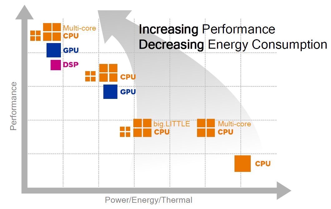
Each of these cores have their own pros and cons. GPUs are excellent at performing parallel processes, while a DSP can crunch numbers faster and while consuming less power than a general CPU, which is efficient at a wide range of other more general tasks.
While heterogeneous compute isn’t going to make much of a difference to checking email and browsing Facebook, it’s an increasingly important part of optimizing the performance of compute heavy tasks, ranging from image and voice processing to playing games in virtual reality. It’s also hugely important for machine learning tasks, which are powering emerging technologies in facial recognition and even virtual reality. While machine learning is often talked about in terms of cloud data, there are also real-time use cases that require on device compute power, but mobile devices have to be efficient to keep within their thermal and power budgets.
As an example, always-on voice recognition assistance can be processed on the lower power DSP, before using the CPU to execute a chosen command or open up an app. Picture quality can be improved by using the ISP and DSP to scan the scene in an image in a small power budget, while making use of the GPU to quickly apply post-processing to the picture.
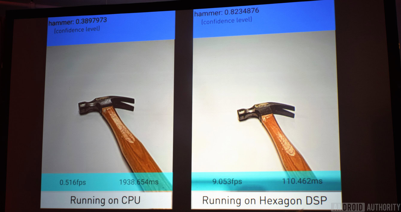
In addition to its new Symphony Manager, Qualcomm also supports Caffe’s neural network framework with the Snapdragon 820, and the Snapdragon 835 introduces compatibility with the open source TensorFlow platform as well. Support for these APIs will allow developers to deploy efficient computation across CPU, DSP and GPU components without having to spend their own development resources working right next to the metal.
Wrap up
The Snapdragon 835 is another notable generational leap for Qualcomm, and not just in terms of performance or the move to another cutting edge manufacturing process. There have been improvements across the board for better display, camera, and graphics technologies. But most importantly, the Snapdragon 835 sets the tone for the next evolution in mobile processing, the move to machine learning and heterogeneous compute. Efficiency is key in the mobile space, and Qualcomm is looking to new techniques to eke out even more performance and power conservation from mobile’s limited 5W budget.