Affiliate links on Android Authority may earn us a commission. Learn more.
What is cache memory - Gary explains
System-on-a-Chip (SoC) designers have a problem, a big problem in fact, Random Access Memory (RAM) is slow, too slow, it just can’t keep up. So they came up with a workaround and it is called cache memory. If you want to know all about cache memory then read on!
You may think it strange to hear that RAM is slow, you might have heard that hard disks are slow, CDROMs are slow, but main memory, are you serious? Of course, speed is relative. We might say that a certain type of road car is the fastest, but then it is relatively slow when compared to a Formula 1 racing car, which itself is slow compared to a supersonic jet and so on.
At the heart of a System-on-a-Chip is the CPU. It rules supreme and it is very demanding. The average mobile CPU is clocked at anywhere from 1.5 GHz to around 2.2GHz. But the average RAM module is clocked at just 200MHz. So what that means is that the average bank of RAM is running with a clock speed that is a factor of 10 slower. For the CPU this is an eon. When it requests something from RAM it has to wait and wait and wait while the data is fetched, time in which it could be doing something else, but can’t as it needs to wait…
OK, I will admit, that is a bit of an over simplification, however it does show us the heart of the problem. The situation isn’t actually that bad because of technologies like Double-Data-Rate (DDR) RAM which can send data twice per clock cycle. Likewise specifications like LPDDR3 (Low Power DDR3) allow for a data transfer rate eight times that of the internal clock. There are also techniques which can be built into the CPU which ensure that the data is requested as early as possible, before it is actually needed.
At the time of writing the latest SoCs are using LPDDR4 with an effective speed of 1866MHz, so if the CPU is clocked at 1.8GHz or less the memory should keep up, or does it? The problem is that modern processors uses 4 or 8 CPU cores, so there isn’t just one CPU trying to access the memory, there are 8 of them and they all want that data, and they want it ASAP!
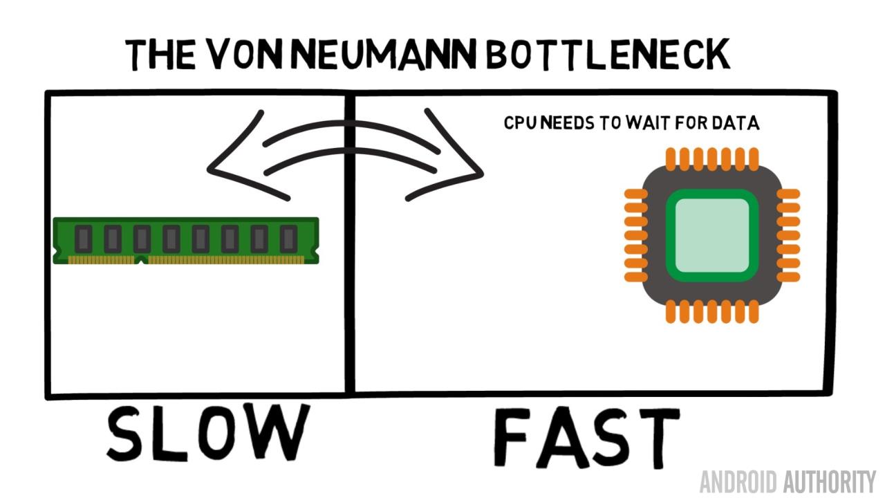
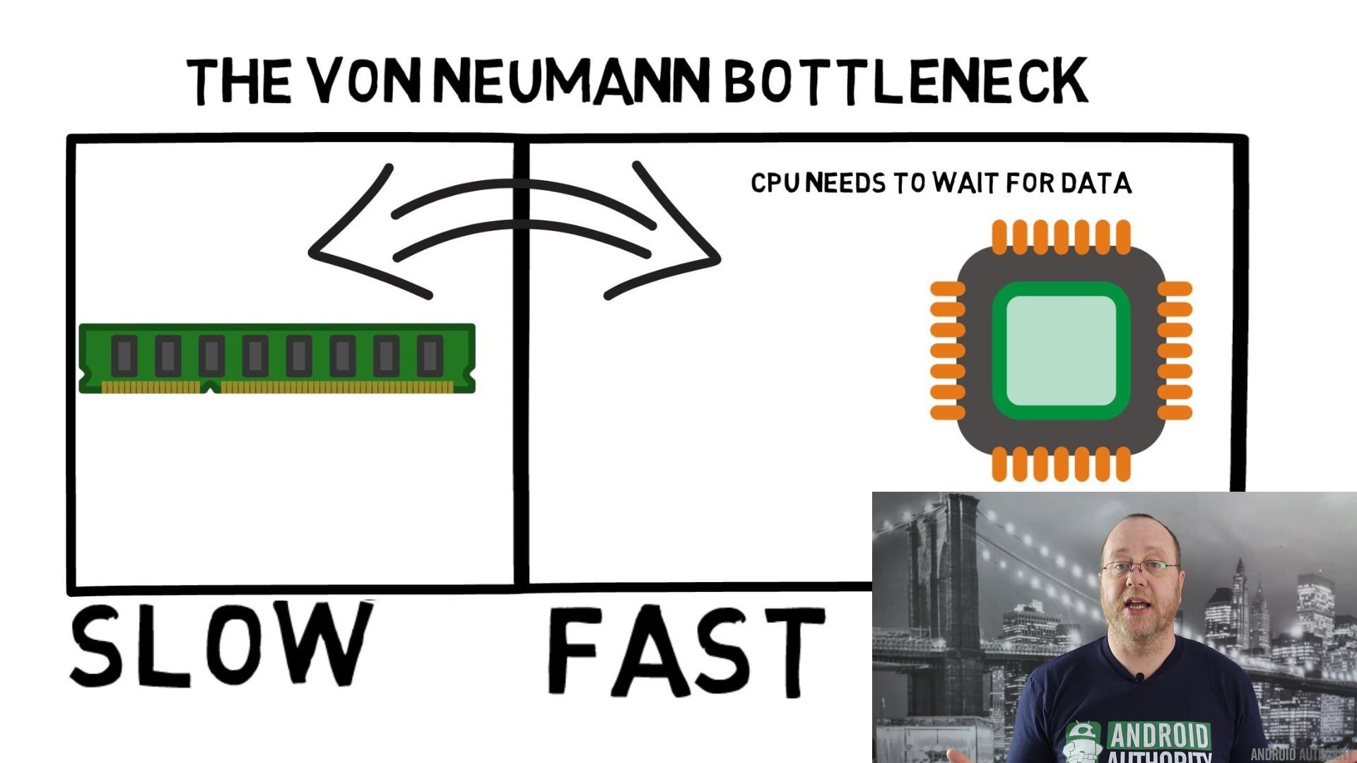
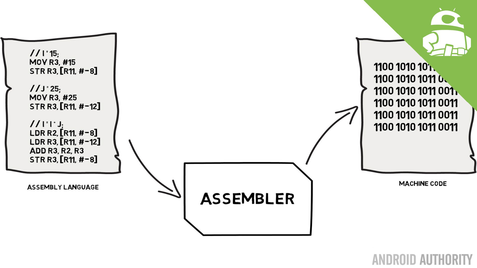
This performance limitation is known as the Von Neumann bottleneck. If you watched my assembly language and machine code video you will remember that Von Neumann was one of the key people in the invention of the modern day computer. The downside of the Von Neumann architecture is the performance bottleneck which appears when the data throughput is limited due to the relative speed differences between the CPU and the RAM.
There are some methods to improve this situation and decrease the performance differential, one of which is the use of cache memory. So what is cache memory? Put simply it is a small amount of memory that is built into the SoC that runs at the same speed as the CPU. This means that the CPU doesn’t need to wait around for data from the cache memory, it is sent over to the CPU at the same speed that the CPU operates. Moreover the cache memory is installed on a per CPU core basis, that means that each CPU core has its own cache memory and there won’t be any contention about who gets access to it.
I can hear you thinking it now, why not make all memory like cache memory? The answer is simply, cache memory that runs at that speed is very expensive. Price (and to some extent the limitations of the fabrication technology) is a real barrier, that is why on mobile the average amount of cache memory is measured in Kilobytes, maybe 32K or 64K.
So, each CPU core has a few Kilobytes of super fast memory which it can use to store a copy of some of the main memory. If the copy in the cache is actually the memory that the CPU needs then it doesn’t need to access the “slow” main memory to get the data. Of course, the trick is making sure that the memory in the cache is the best, the optimal, data so that the CPU can use the cache more and the main memory less.
[related_videos title=”Latest Reviews:” align=”center” type=”custom” videos=”682235,680816,680369,679646″]
Since it only has a few Kilobytes of cache memory available there will be times when the cache has the right memory contents, known as a hit, and times when it doesn’t, known as a miss. The more cache hits the better.
Split caches and hierarchy
To help improve the number of hits versus misses there are a number of techniques which are used. One is to divide the cache in two, one for instructions and one for data. The reason to do this is that filling an instruction cache is much easier, since the next instruction to be executed is probably the next instruction in the memory. It also means that the next instruction to be executed can be fetched from the instruction cache while the CPU is also working on memory in the data cache (since the two caches are independent).
[related_videos title=”Top flagships of 2016″ align=”center” type=”custom” videos=”676936,684612,682146,675002″]
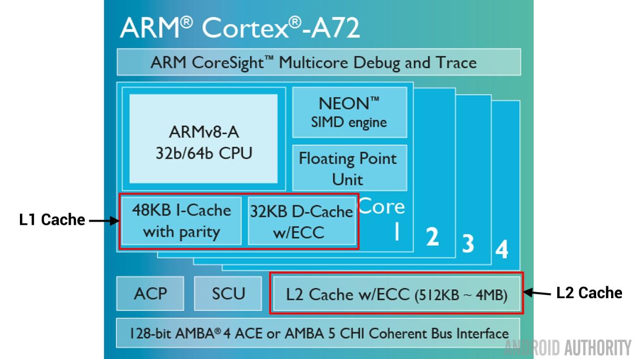
Another technique to improve overall cache hits is to use a hierarchy of caches, these are traditionally known as L1 (level 1) and L2 (level 2) caches. L2 is normally a much larger cache, in the Megabyte range (say 4MB, but it can be more), however it is slower (meaning it cheaper to make) and it services all the CPU cores together, making it a unified cache for the whole SoC.
The idea is that if the requested data isn’t in the L1 cache then the CPU will try the L2 cache before trying main memory. Although the L2 is slower than the L1 cache it is still faster than the main memory and due to its increased size there is a higher chance that the data will be available. Some chip designs also use a L3 cache. Just as L2 is slower but larger than L1, so L3 is slower but larger than L2. On mobile L3 cache isn’t used, however ARM based processors which are used for servers (like the upcoming 24-core Qualcomm server SoC or the AMD Opteron 1100) have the option of adding a 32MB L3 cache.
Associativity
There is one more piece in the cache memory jigsaw. How does the CPU know where the contents from main memory is stored in the cache? If the cache was just a long list (a table) of cached memory slots then the CPU would need to search that list from top to bottom to find the contents it needs. That, of course, would be slower than fetching the contents from main memory. So to make sure that the memory contents can be found quickly a technique known as hashing needs to be used.
A hash function takes a value (in this case the address of the memory contents being mirrored in the cache) and generates a value for it. The same address always generates the same hash value. So the way the cache would work is that the address is hashed and it gives a fixed answer, an answer that fits within the size of the cache, i.e. 32K). Since 32K is much smaller than the size of RAM, the hash needs to loop, which means that after 32768 addresses the hash will give the same result again. This is known as direct mapping.
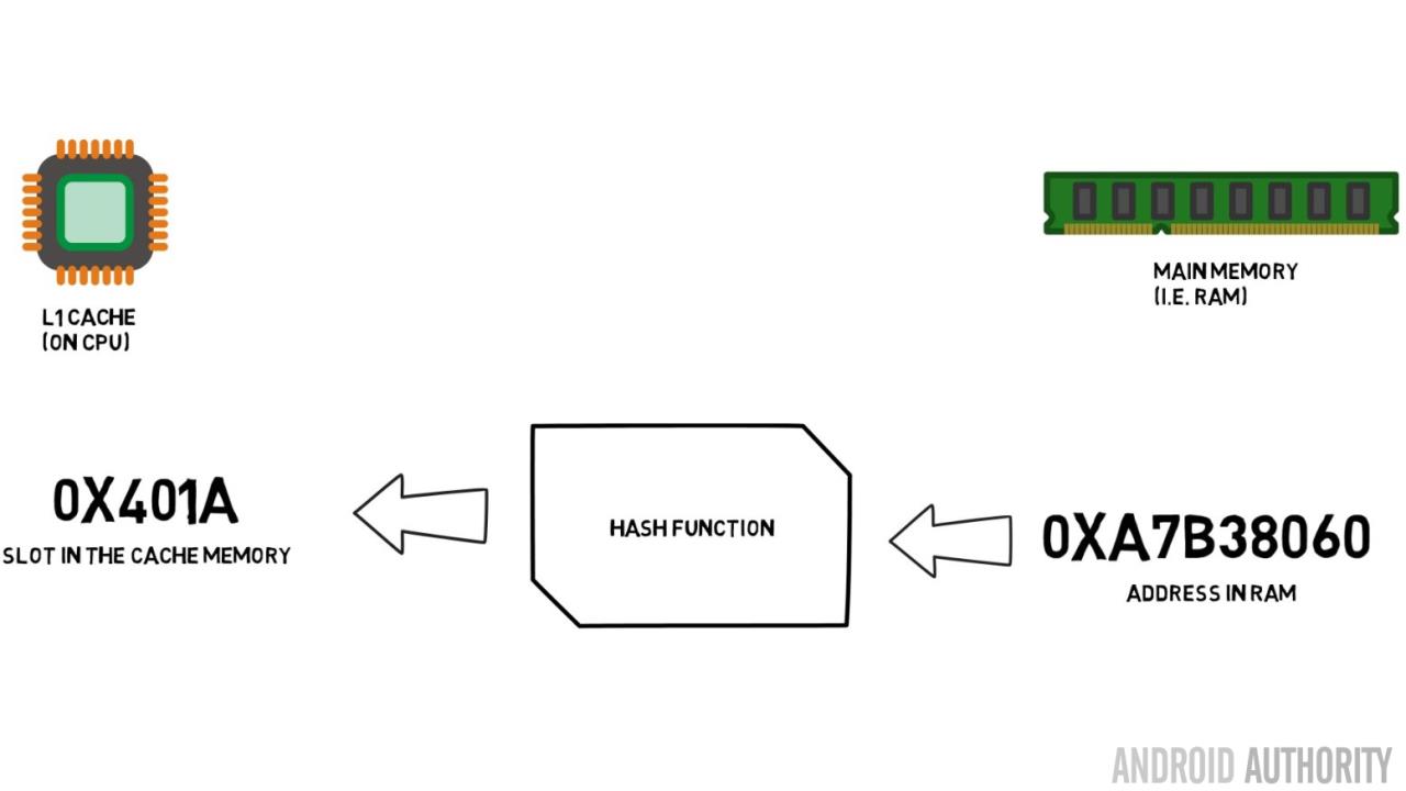
The downside of this approach can be seen when the contents of two addresses need to be cached but the two addresses return the same cache slot (i.e. they have the same hash value). In such situations only one of the memory locations can be cached and the other remains only in main memory.
Another approach is to use a hash which works in pairs, so any address can be one of a pair of locations in the cache, i.e. hash and hash+1. This means that two addresses which previously would have clashed, as they had the same hash, can now co-exist. But to find the right slot in the cache the CPU needs to check 2 locations, however that is still much faster than searching 32768 possible locations! The technical name for this mapping is called 2-way associative. The associative approach can be extended to 4-way, 8-way, and 16-way, however there are limits where the performance gains don’t warrant the extra complexity or costs.
[related_videos title=”Gary Explains:” align=”center” type=”custom” videos=”682738,681421,678862,679133″]
Wrap-up
There is a performance bottleneck inside of every System-on-a-Chip (SoC) do to the difference in speed of the main memory and the CPU. It is known as the Von Neumann bottleneck and it exists just as much in servers and desktops as it does in mobile devices. One of the ways to alleviate the bottleneck is to use cache memory, a small amount of high performance memory that sits on the chip with the CPU.
Thank you for being part of our community. Read our Comment Policy before posting.