Affiliate links on Android Authority may earn us a commission. Learn more.
🧊 Good morning! It's snowing here in Berlin. In May. Good times.

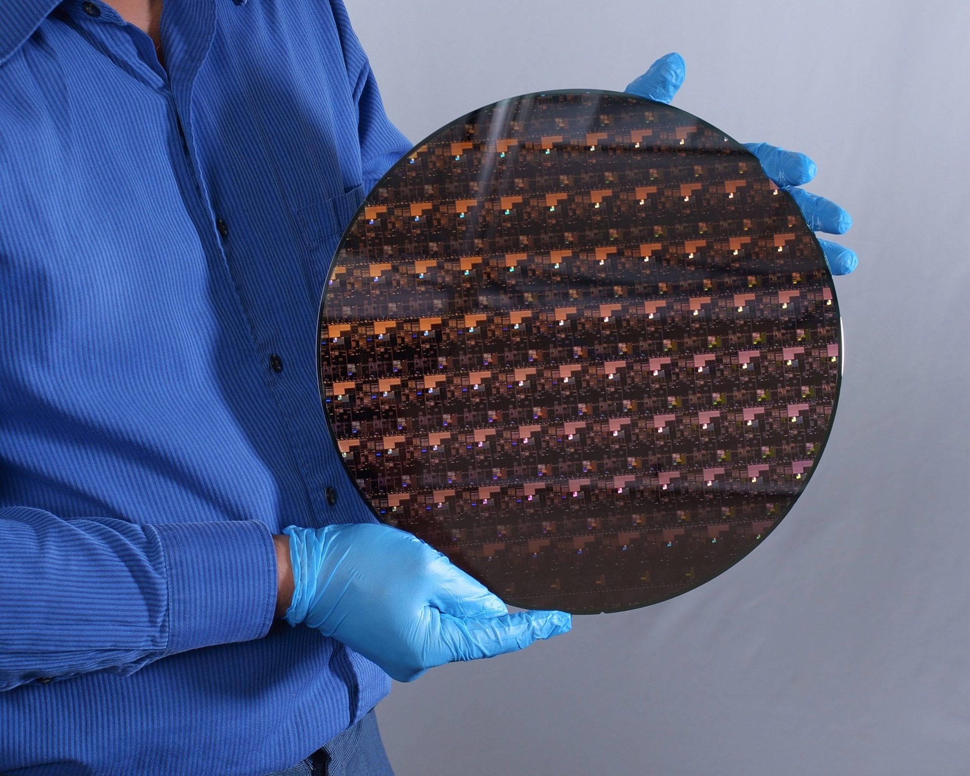
IBM isn’t a semiconductor foundry, but it is one of the world’s leading research bases for semiconductor breakthroughs.
- IBM, the company is quick to point out, was the first research institution to demonstrate 7nm chips in 2015 and 5nm in 2017.
- Yet IBM doesn’t make chips itself — it sold off the business in 2014.
- Rather than spend billions on manufacturing facilities itself, IBM licenses its IP and production methods to foundries including Samsung, and recently, Intel, for their production processes.
The 2nm breakthrough:

Now comes what IBM calls 2 nanometer chips, which are a breakthrough but not necessarily related to the actual dimensions of the transistors on the wafer, but the density.
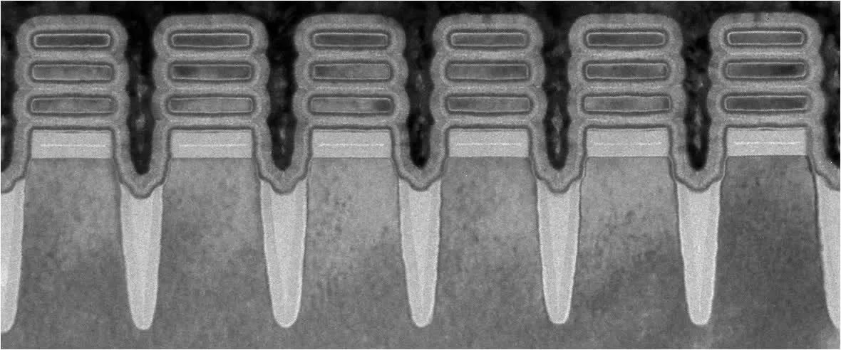
- That’s due to the evolution over previous chip eras, as the designs are now 3D.
- IBM has made its chips taller: now 75nm tall.
AnandTech is, of course, your place to go, and its article is superb in breaking down the marketing speak into closer to real-world details.
For example:
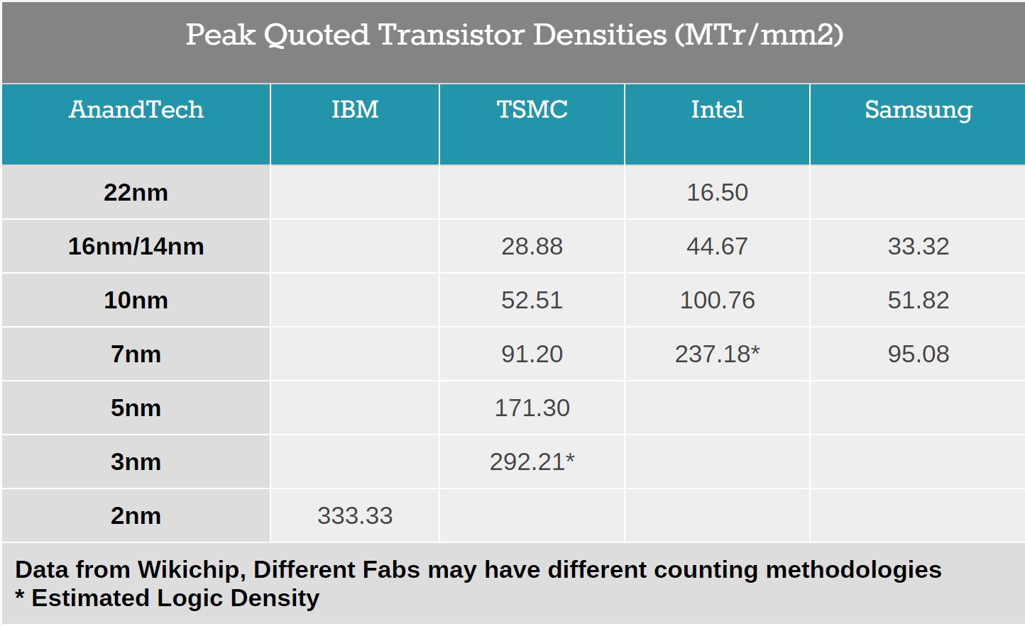
- “IBM states that the technology can fit ’50 billion transistors onto a chip the size of a fingernail’. We reached out to IBM to ask for clarification on what the size of a fingernail was, given that internally we were coming up with numbers from 50 square millimeters to 250 square millimeters. IBM’s press relations stated that a fingernail in this context is 150 square millimeters. That puts IBM’s transistor density at 333 million transistors per square millimeter (MTr/mm2).
Here’s AnandTech’s table of the world’s leading foundries and their processes at different quotes sizes:

- Wired does a good job of simplifying what 3D means, here:
- “Making the new transistor relies on not simply etching the features of a chip into silicon, but also building them on top of one another. Chipmakers first began crafting transistors in three dimensions in 2009 using a design called FinFET, in which electrons flow through thin vertical fins—rather than a flat surface—to pass through transistors. The IBM design takes this further, stacking transistors on top of one another in the form of nanosheets that run through a semiconducting material like the layers in a cake.”
When do we get the benefits?
- IBM says the new chip breakthrough projects to “achieve 45 percent higher performance, or 75 percent lower energy use, than today’s most advanced 7 nm node chips.”
- That, very loosely, could mean for your given laptop or smartphone that lasts a day on battery, you might get as many as four days out of a charge, though a lot depends on the display.
- We might see this as a leading standard in flagships chipsets and devices perhaps by 2023 or 2024.
🔒 On World Password Day, Google reveals that 2FA will eventually be mandatory (Android Authority).
🔀 Here’s how WhatsApp’s multi-device syncing feature could work (Android Authority).
📁 Oppo is testing a clamshell foldable phone, no clues as to how far along development this is (Android Authority).
🎮 Nintendo warns that Switch consoles are about to get even harder to find, thanks to the ol’ chip shortage again (Android Authority).
🔊 The Google Assistant is now a Google messaging service, with “Broadcast” now working on speakers, displays, and phones (Ars Technica).
⚖ More out of Epic vs Apple: Apple made it harder to change Hulu subscriptions because of a tweet
📸 Sony ditches DSLRs, moving the camera industry beyond film-era designs to mirrorless (CNET).
📺 Netflix is considering launching N-Plus, a behind-the-scenes content hub (TNW).
♻ Microsoft is finally ditching its Windows 95-era icons (The Verge).
🤔 “Why I work on ads” (jefftk.com/)
🎈 High Hopes claims stratospheric breakthrough in direct air CO2 capture: launch hot air balloons to capture more carbon (New Atlas).
🌠 “Why are 75% of the earth’s annular lakes north of the 49th parallel when only about 1/8 of the earth’s land surface is there?” (r/askscience)

I’m sorry to report that critics aren’t too fussed about what I thought sounded very fun: a new pizza vending machine. In Rome. Italy. (You’d think they’d try something like this where the pizza isn’t such a religion?)
Anyway:
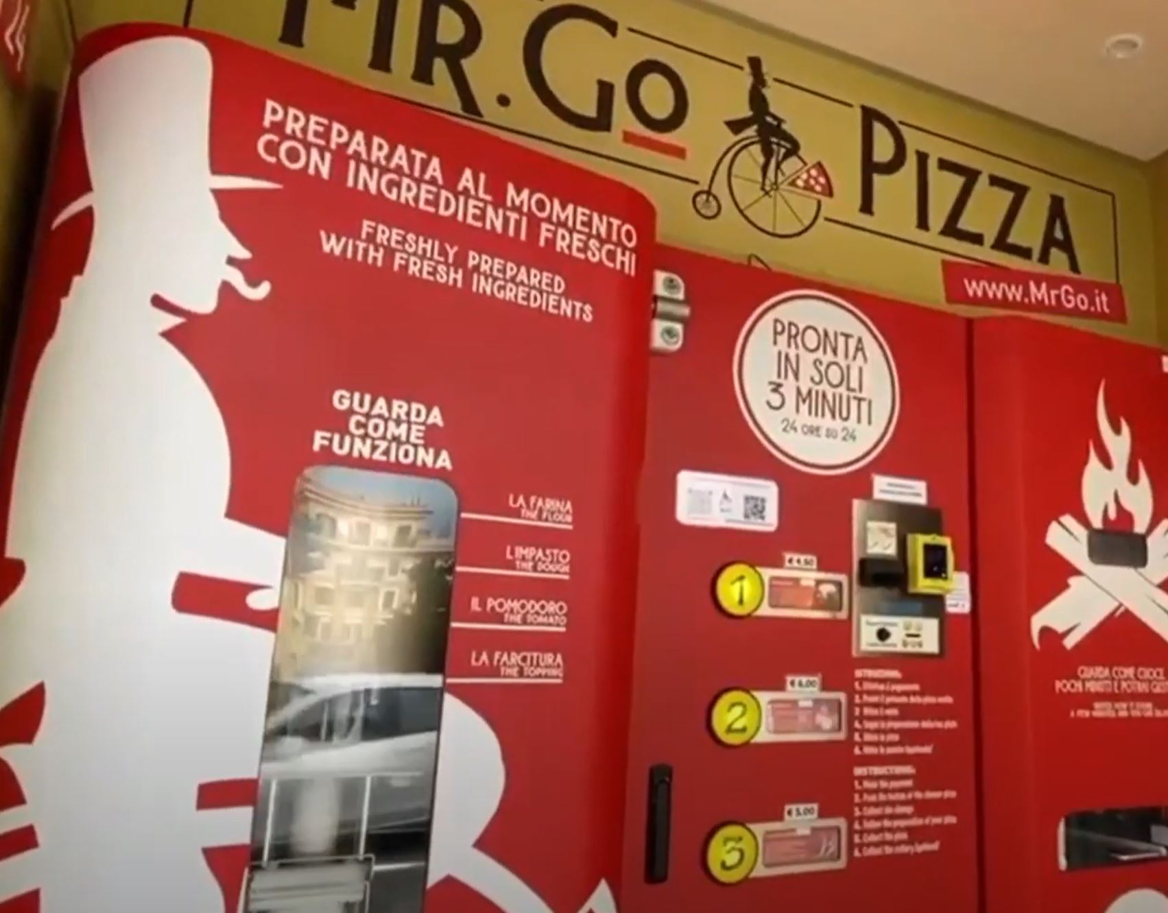
- A Mr. Go Pizza vending machine looks to be about three times as wide as a regular old drink vending machine, and was recently installed in Piazza Bologna in Rome. It promises to cook four types of pizza for about $5-$7.
- Happily, it’s visual too — the machine kneads the pizza base and adds toppings and cooks it all with little viewing windows.
However. Reuters reports, surprise surprise, it isn’t going well:
- Customer reviews “ranged from “acceptable if you’re in a hurry” to outright horror.”
- “It looks good but it is much smaller than in a restaurant and there is less topping,” said Claudio Zampiga, a pensioner.
- “It’s OK but it’s not pizza,” said one student, who described the taste as more like a “piadina,” a super-thin soft unleavened bread wrap popular in northern Italy, than a pizza.
Here’s a video of it in action. Auto-translate seems to say the guy thinks it’s probably ok if you’re rolling past it at 2am and need a slice.
Say what you want, but nothing about this doesn’t make me hungry!
Have a great weekend,
Tristan Rayner, Senior Editor.

