Affiliate links on Android Authority may earn us a commission. Learn more.
Tegra X1 - a closer look at NVIDIA's "superchip"
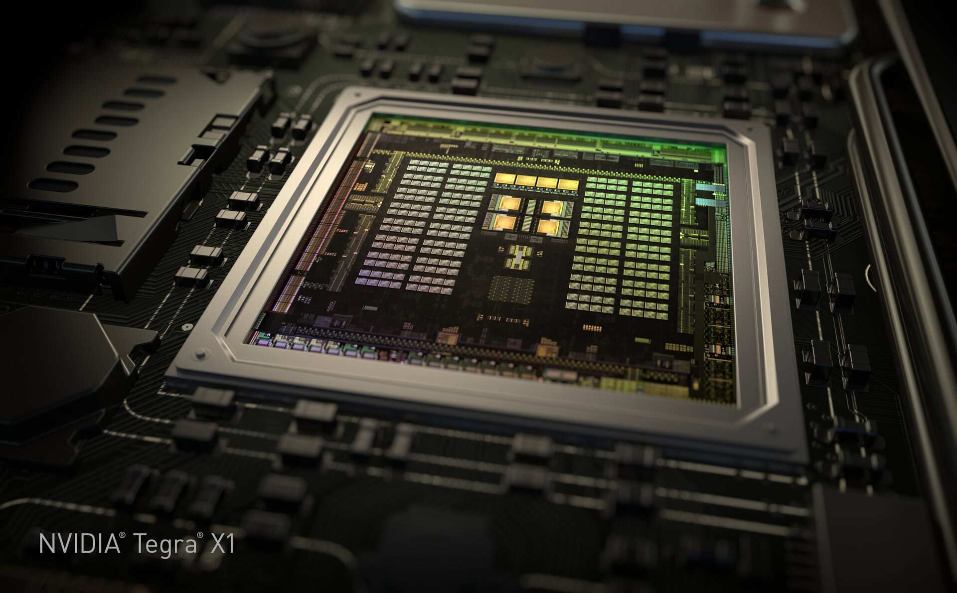
One of the first announcements out of CES 2015 was Nvidia’s new Tegra X1 SoC, the graphics giant’s successor to its rather good Tegra K1. Featuring the latest powerhouse ARM Cortex-A57 and A53 CPU combo and NVIDIA’s Maxwell GPU technology, the company’s first 20nm SoC looks to be as energy efficient as it is powerful. Let’s delve a little deeper into what the NVIDIA Tegra X1 has to offer.
CPU
The first thing you’ll probably have noticed about the Tegra X1 is that NVIDIA appears to have ditched its customized 64-bit Denver CPU architecture, as found in the Nexus 9’s Tegra K1, and has gone back to a more standard 64-bit ARM configuration. That is not to say this chip isn’t interesting, NVIDIA will be among the first to bring an octa-core Cortex A57 and A53 SoC, arranged in two groups of four, to market. This design is similar to Qualcomm’s upcoming Snapdragon 810 and Samsung’s existing Exynos 5433.
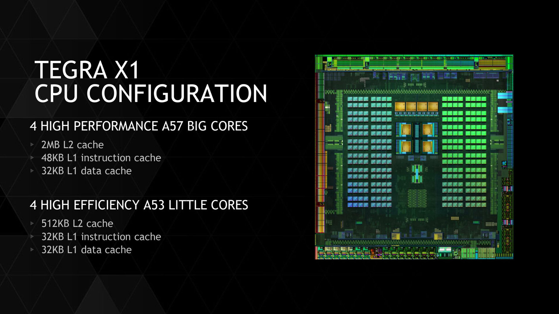
There are a couple of reasons why NVIDIA may have chosen to go back to ARM’s designs. NVIDIA itself stated that time-to-market is the leading reason, suggesting that shrinking its Denver CPU design down to 20nm was more time consuming than picking up and tweaking an ARM design. Alternatively, perhaps NVIDIA wasn’t convinced by the performance results of its custom CPU, although it has hinted that Denver may reappear in a future SoC. Regardless, let’s take a look at what NVIDIA has done with ARM’s reference designs.
The high-end A57 CPU cluster has 2MB of L2 cache shared across the four cores, along with 48KB L1 instruction and 32KB L1 data caches. The four energy efficient A53 CPUs share 512KB of L2 cache and have two 32KB L1 caches for instructions and data.
As the multiple CPU core design suggests, NVIDIA’s chip operates as a big.LITTLE design in order to more efficiently share workloads across the most appropriate CPU cores. However, NVIDIA has opted for its own custom interconnect, rather than ARM’s CCI-400, and cluster migration, rather than global task scheduling, to open up all eight cores for use at once.
NVIDIA touts that its interconnect design significantly outperforms Samsung’s System LSI used in the Exynos 5433, boasting 1.4 times more performance for the same amount of power or half the power required to produce the same level of performance. This is partially down to cache coherence, which reduces the power/performance penalties usually associated with cluster migration. NVIDIA has also decided to use its own System Electrical Design Point power management system to throttle and gate clock speeds, rather than ARM’s in-house Intelligent Power Allocation feature.
Although the Tegra X1 has gone back to an ARM CPU design, NVIDIA clearly believes that its own customizations can improve on the standard ARM formula.
GPU
New technology also makes its way into the GPU aspect of NVIDIA’s latest SoC. The Tegra X1 again features NVIDIA’s proprietary graphics architecture, although this time the SoC is packing the company’s latest Maxwell architecture, which powers the high-end GTX 980 range of graphics cards, as well as the incredibly power efficient GTX 750Ti.
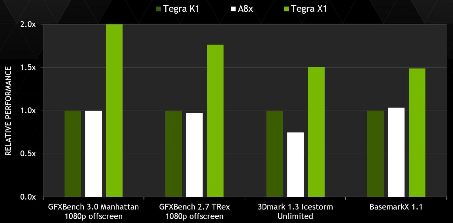
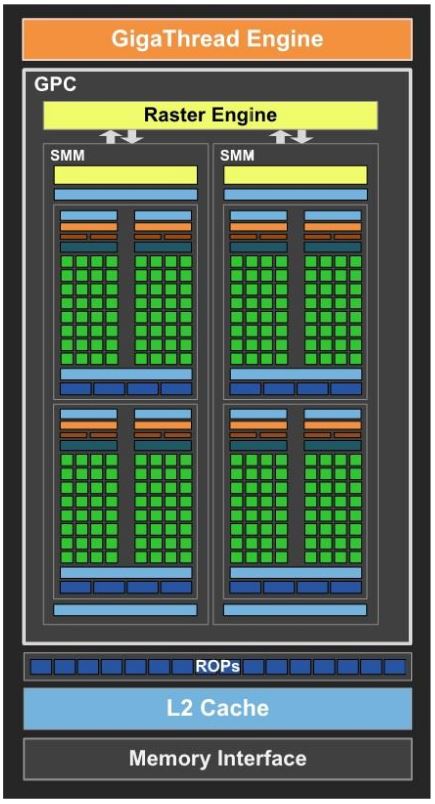
NVIDIA claims to have doubled the GPU performance and halved the chip’s power requirements compared with the Tegra K1. NVIDIA’s benchmarks suggest that this energy efficiency has been ploughed straight back into increasing performance, meaning that the X1’s GPU is still likely to be quite power hungry. Just like the Tegra K1, the X1 is probably destined for tablet products, where manufacturers can squeeze in some extra battery capacity.
The GPU design has changed a little compared with last generation, featuring two Maxwell SMMs (Streaming Multiprocessors) for a total of 256 CUDA cores, compared with a single Kelper SMX and 192 CUDA cores in the Tegra K1. Although the number of CUDA cores may not have doubled up, NVIDIA states that a Maxwell SMM is up to 40 percent more efficient than an older Kepler SMX. Furthermore, the move to two complete SMMs means that important geometry and textures units have been doubled.
NVIDIA has also quadrupled the number of ROPs to 16 and has added a 256KB L2 cache between the ROPs and the 64-bit memory interface, which should help the GPU drive those higher resolution displays. General memory improvements will also play a big part in the Tegra X1’s performance leaps at higher resolutions, as this is generally an area in which mobile devices suffer from bottlenecks.
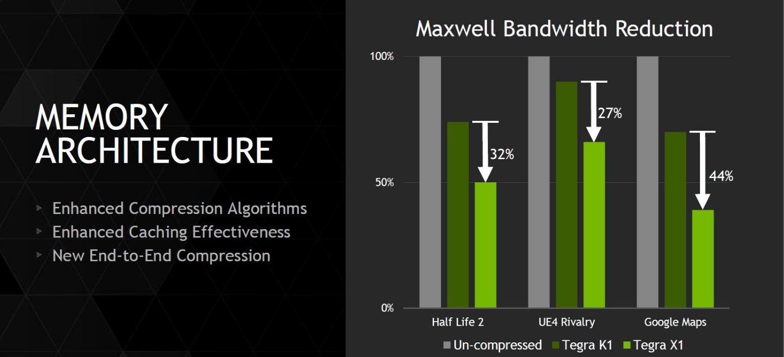
Speaking of memory, NVIDIA has also implemented a new and improved memory compression features in the Tegra X1, to further alleviate DRAM bandwidth demands on the chip’s 64-bit memory bus. The GPU continues to support a range of OpenGL 4.x and DirectX 11.x features, including Tessellation, Tiled Resources and Voxel Global Illumination, ensuring that NVIDIA mobile customers can make the most of the latest gaming effects and efficiencies.
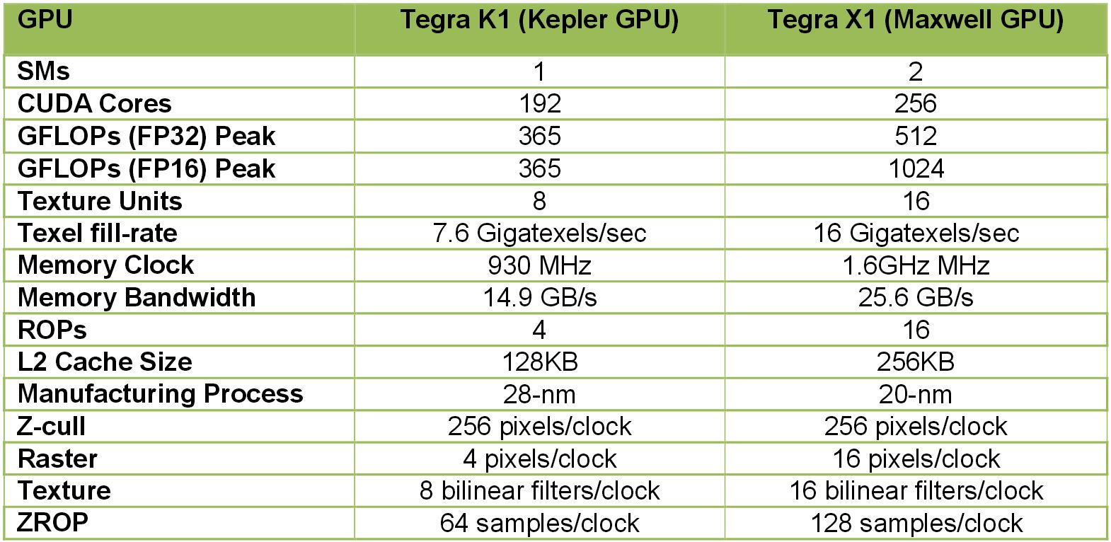
One final important feature added to the Tegra X1 is support for “double speed FP16” (16-bit floating point operations) in the GPU’s CUDA cores. Typically Maxwell only features FP32 and FP64 cores, but NVIDIA has altered FP16 operation handling in the X1, whereby a limited set of FP16 operations can be packed together and computed over a single FP32 core. This is not ideal, but will allow NVIDIA to compete with its rivals in situations where FP16 operations are important. Overall, these changes add up to 1024 GFLOPs (1 TFLOP) FP16 performance and 512 GFLOPs for FP32 operations.
Feature Set
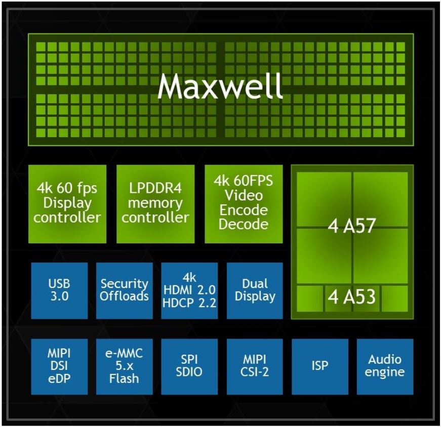
NVIDIA hasn’t just gone all-out with its CPU and GPU design. Tying the whole SoC together is a 64-bit wide LPDDR4 memory interface that supports up to 4GB of RAM. Peak memory bandwidth has been boosted up to 25.6 GB/s, up from 14.9GB/s and energy efficiency has improved by around 40 percent. The Tegra X1 now supports eMMC 5.1 memory for faster reading and writing of high speed storage cards.
Video and display support has also been bumped up this generation. The Tegra X1 supports 60fps 4K H.265, H.264, VP9 and VP8 video encode and decode, improving on the 30fps 4K limit of the Tegra K1. External displays are now also supported at 60fps for 4K video content via HDMI 2.0 and HDCP 2.2 connections. JPEG encode and decode has also received a fivefold speed boost, up from 120 MP/s to 600 MP/s, although the other ISP features appear the same as the Tegra K1. The Dual ISP supports 4096 focus points, 100 MP sensors and up to 6 camera inputs.
Sum-up
The Tegra X1 is a clear improvement over its predecessor and should provide a considerable jump in GPU performance. As Qualcomm, Samsung and MediaTek all move over to new ARM Cortex CPU designs this year, NVIDIA is banking on its graphics prowess to set it apart from the competition. We will have to wait to get our hands on the chip to know for sure if the Tegra X1 has what it takes to challenge the mobile market’s biggest players, but NVIDIA’s latest effort certainly looks like a strong contender this year.